Motivation
This is a derivation off the ADSR for my NGF-E project. Because this one is a stand alone module I have removed all additional features from the Next Generation Formant project. Nonetheless it is still based on original Elektor Formant ADSR schematic. I made some error corrections and added my changes to the design. All parts are updated to today (2017/10) available parts. I have made a few changes to fix some shortcomings of the original. A triple range switch was added for finer adjustment of the ADSR CV-output signal. The attack rise time is shorter now as in the original. The gate input is buffered. The fixes a fault in the original when working with analog sequencers. A manual single shot is added. This comes in handy while testing patches and in live performance. The output voltage is slightly raised to reach really 5V. Due to the design of the original Elektor Formant ADSR the output of the original ADSR keeps a residual voltage of about 0,5V. I have put an (adjustable) compensation in my design to correct this and keep the original behavior if needed as well. The driver circuitry for the output indicator LED is changed for better linearity.
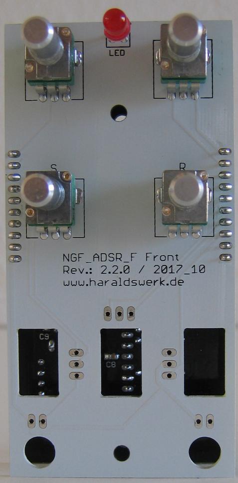
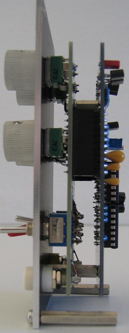
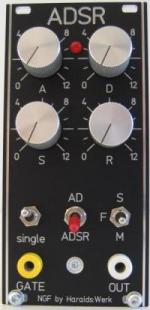
Most noticeable change is moving to a "flat" design. The depth of the module is reduced and most important no more potentiometer wiring is needed!
Specs and features
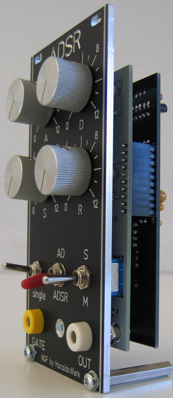
- AD/ADSR switch
- Gate input 5V
- Gate manual single shot
- CV output ~0..5V
- CV output indicator
- Range switch: fast, middle, long
- Attack (A) 0,5ms...16s
- Decay (D) 4ms...40s
- Sustain (S) 0..5V
- Release (R) 4ms..40s
- Runs on +/-15V and +/-12V (with minor resistor value changes)
- Schematic ADSR
- Pictures
- Download docs
Implementation
Schematic
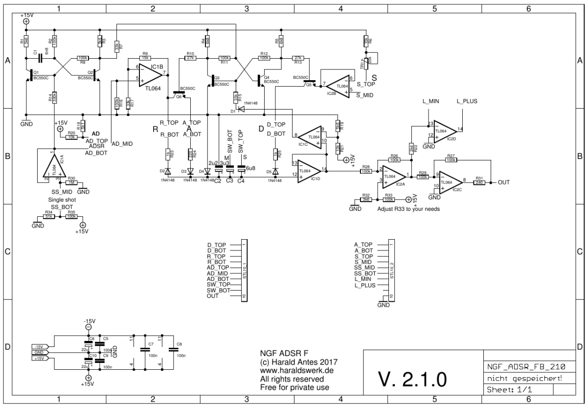
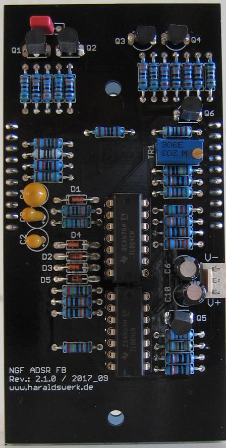
NGF ADSR schematic back PCB
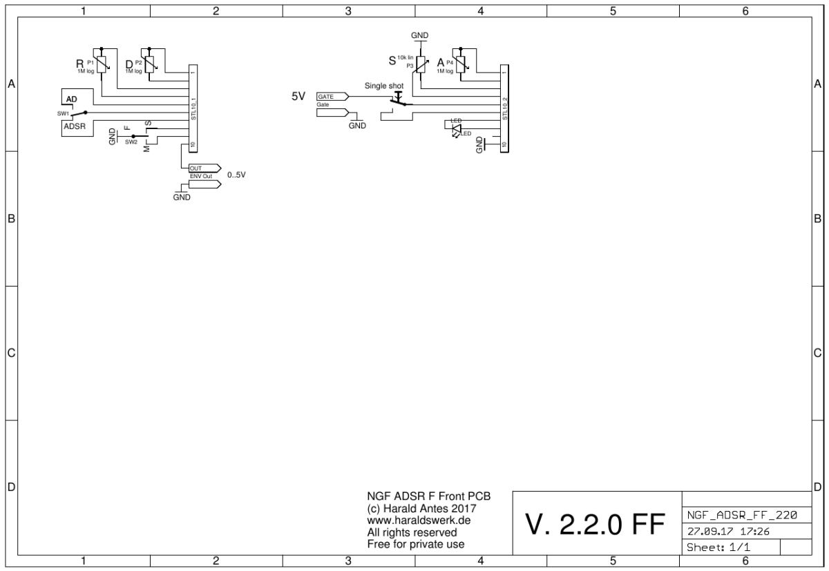
NGF ADSR schematic front PCB
Description:
This is a close clone of the Elektor Formant ADSR. Here i only describe the changes i have made. The description of the other parts of the circuitry can be found in the original Elektor Formant documentation. The gate signal input resistance is raised from 33kOhm to 1megOhm with the input buffer IC1A. This protects against double triggering with the falling edge of the gate signal when using sequencers. R30 is used to fix the input to a defined potential when no signal is attached to the input. R34 and R35 in combination with a push button give you the single shot feature. C1 was lowered to 6n8 from 10nF. In combination with C2 and the raised charging voltage through IC1B/R9 this makes for faster attack time. The load capacitor of 10u was replaced with three selectable capacitors of 2,2uF 3,3uF and 6,8uF. This make for a finer adjustment of the response times of the ADSR. The voltage divider R19/R21 was adjusted to ensure that the output level of 5V is reached when the offset option with R32/R33 is used. If this feature is not used R25 should be lowered to 5k1. Construction conditioned the output at IC1D only reaches a minimal voltage of about 0,5V. To compensate for this i added IC2A. With R32/R33 you can trim the output down to zero volts. If the ADSR is not used the output voltage is now at -0,5V. If you don't want to use this feature just leave R33 out and you will have the original behavior of the original Elektor Formant ADSR. The current consumption was lowered with using the TL064 and a low current led.
Calibration
- The calibration of the sustain level with TR1 is done as described in the original documentation.
- With R32/R33 you can compensate for the residual voltage.
Special parts
None