Motivation
This is another derivation off the ADSR for my NGF-E project, adapted to 12V Euro-rack format. Because this one is a stand alone module I have removed all additional features from the Next Generation Formant project. Nonetheless it is still based on original Elektor Formant ADSR schematic. I made some error corrections and added my changes to the design. All parts are updated to today (2021/01) available parts. I have made a few changes to fix some shortcomings of the original. A triple range switch was added for finer adjustment of the ADSR CV-output signal. The attack rise time is shorter now as in the original. You can have a punchy attack with about 0.5mS now. The gate input is buffered. The fixes a fault in the original when working with analog sequencers. The output voltage is slightly raised to reach really 5V. Due to the design of the original Elektor Formant ADSR the output of the original ADSR keeps a residual voltage of about 0,5V. I have put an compensation in my design to correct this. The driver circuitry for the output indicator LED is changed for better linearity.
Specs and features
- AD/ADSR switch
- Gate input 5V
- CV output ..5V
- CV output indicator
- Range switch: fast, middle, long
- Attack (A) 0,5ms...16s
- Decay (D) 4ms...40s
- Sustain (S) 0..5V
- Release (R) 4ms..40s
- Power consumption below 15mA each rail
Implementation
Schematic

ADSR: Main board schematic

ADSR: Control board schematic
Description:
This is a close clone of the Elektor Formant ADSR. Here i only describe the changes i have made. The description of the other parts of the circuitry can be found in the original Elektor Formant documentation. The gate signal input resistance is raised from 33kOhm to 1megOhm with the input buffer IC1A. This protects against double triggering with the falling edge of the gate signal when using sequencers. R30 is used to fix the input to a defined potential when no signal is attached to the input. C1 was lowered to 6n8 from 10nF. In combination with C2 and the raised charging voltage through IC1B/R9 this makes for faster attack time. The load capacitor of 10u was replaced with three selectable capacitors of 2,2uF 4,7uF and 10uF. This makes for a finer adjustment of the response times of the ADSR. The voltage divider R19/R21 was adjusted to ensure that the output level of 5V is reached. If this feature is not used R25 should be lowered to 5k1. Construction conditioned the output at IC1D only reaches a minimal voltage of about 0,5V. To compensate for this i added IC2A. If the ADSR is not used the output voltage is now at -0,5V. The current consumption was lowered with using the TL064 and a low current LED.
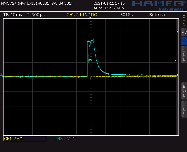
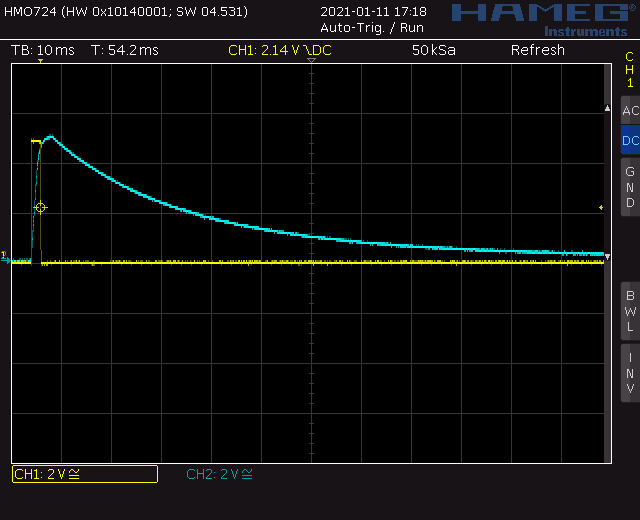
ADSR: Screenshot AD curve fast attack/decay
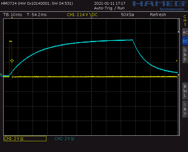
ADSR: Screenshot AD curve slow attack/decay
ADSR: Screenshot AD curve fast attack slow decay
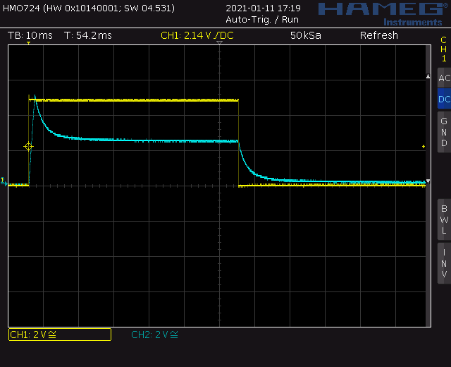
ADSR: Screenshot ADSR curve fast attack/decay/release
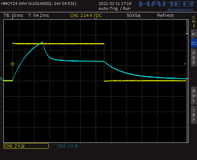
ADSR: Screenshot ADSR curve slower attack/decay/release
Top
Calibration
- The calibration of the sustain level with TR1 is done as described in the original documentation.
Building hints
- None
Special parts
- None
Download
ADSR control board documentation downloadADSR control board Gerber files download
ADSR main board documentation download
ADSR main board Gerber files download
ADSR *.fpd file download
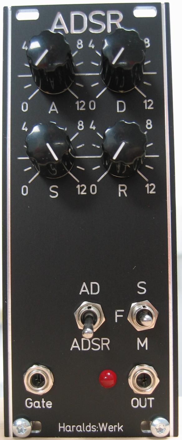
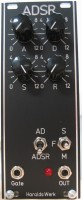
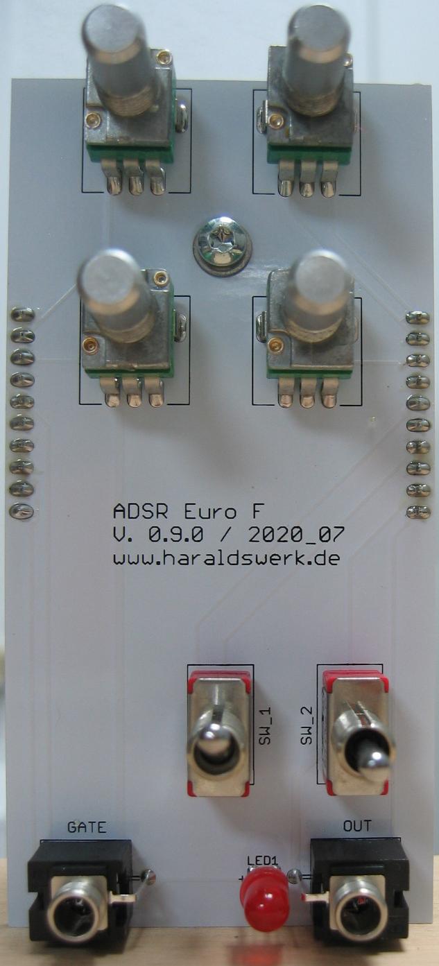
ADSR: Front view
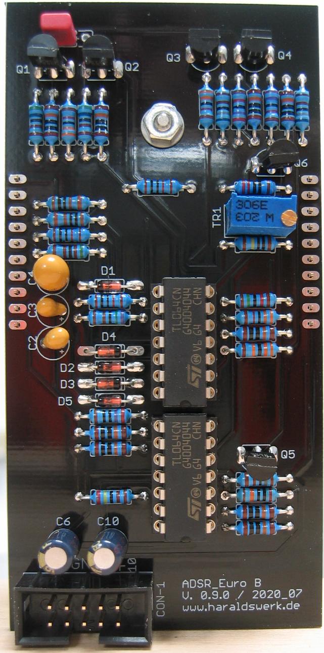
ADSR: Populated control PCB
ADSR: Populated main PCB
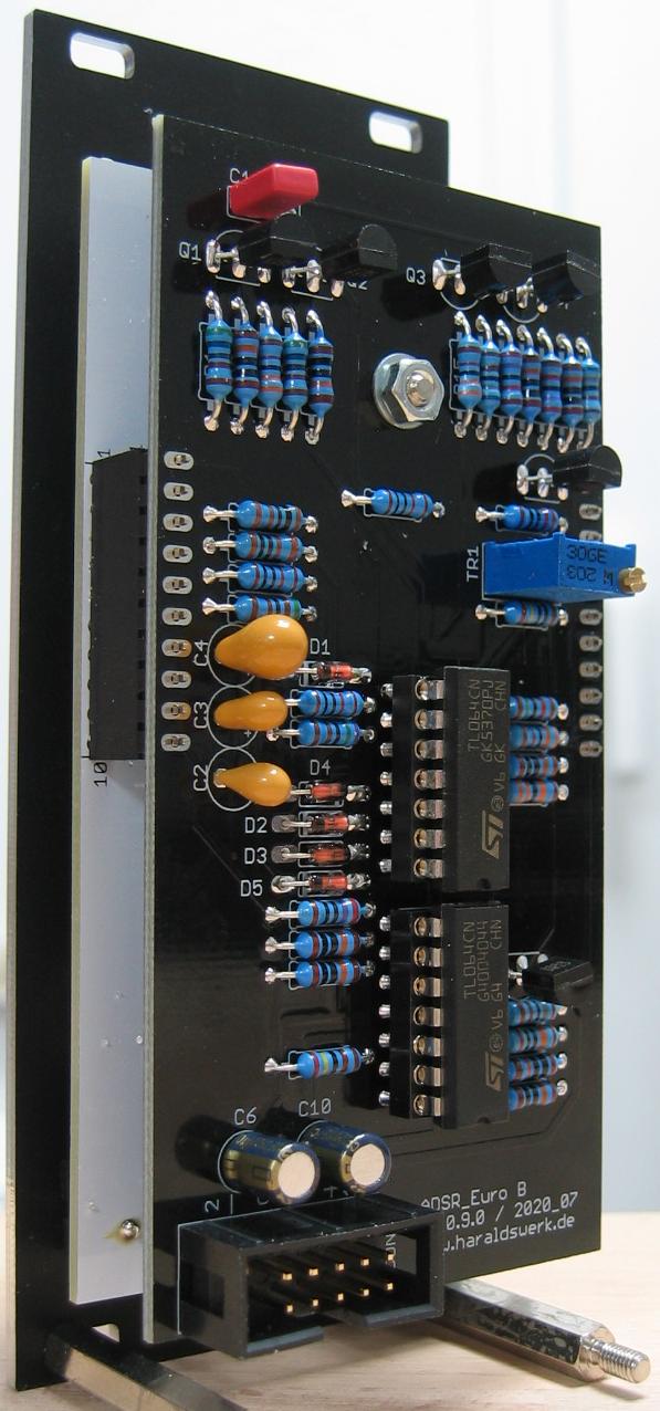
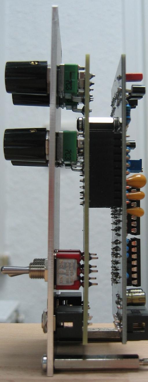
ADSR: Back view